Last week I delved into the science of how film captures an image. This time we’ll investigate the very different means by which electronic sensors achieve the same result.
CCD

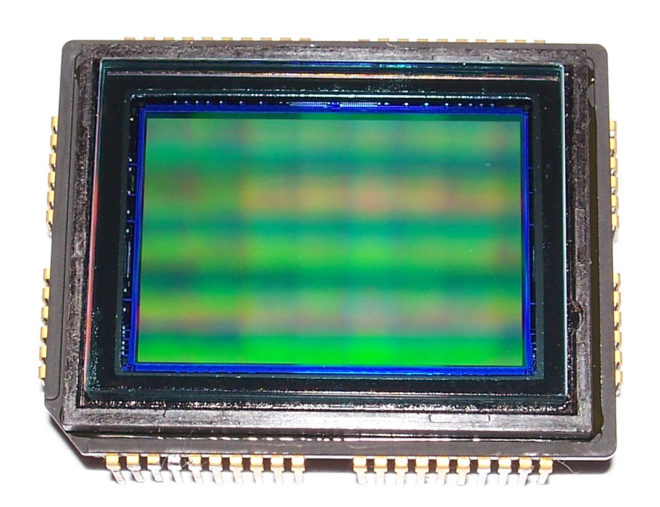
In the twentieth century, the most common type of electronic imaging sensor was the charge-coupled device or CCD. A CCD is made up of metal-oxide-semiconductor (MOS) capacitors, invented by Bell Labs in the late fifties. Photons striking a MOS capacitor give it a charge proportional to the intensity of the light. The charges are passed down the line through adjacent capacitors to be read off by outputs at the edges of the sensor. This techniques limits the speed at which data can be output.
My first camcorder, an early nineties analogue 8mm video device by Sanyo, contained a single CCD. Professional cameras of that time had three: one sensor each for red, green and blue. Prisms and dichroic filters would split the image from the lens onto these three CCDs, resulting in high colour fidelity.
A CCD alternates between phases of capture and read-out, similar to how the film in a traditional movie camera pauses to record the image, then moves on through the gate while the shutter is closed. CCD sensors therefore have a global shutter, meaning that the whole of the image is recorded at the same time.
CCDs are still used today in scientific applications, but their slow data output, higher cost and greater power consumption have seen them fall by the wayside in entertainment imaging, in favour of CMOS.
CMOS

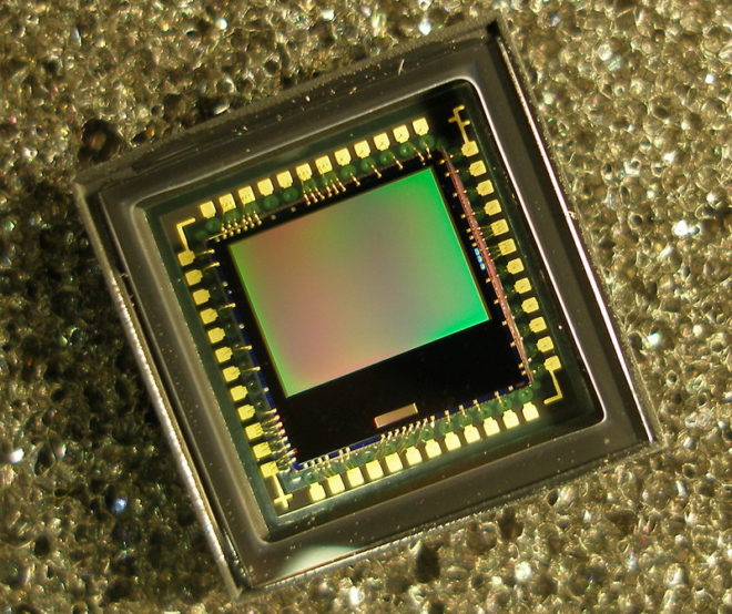
Complementary metal-oxide-semiconductor sensors (a.k.a. APS or active-pixel sensors) have been around just as long as their CCD cousins, but until the turn of the millennium they were not capable of the same imaging quality.
Each pixel of a typical CMOS sensors consists of a pinned photodiode, to detect the light, and a metal-oxide-semiconductor field-effect transistor. This MOSFET is an amplifier – putting the “active” into the name “active-pixel sensor” – which reduces noise and converts the photodiode’s charge to a voltage. Other image processing technology can be built into the sensor too.
The primary disadvantage of CMOS sensors is their rolling shutter. Because they capture an image row by row, top to bottom, rather than all at once, fast-moving subjects will appear distorted. Classic examples include vertical pillars bending as a camera pans quickly over them, or a photographer’s flash only lighting up half of the frame. (See the video below for another example, shot an iPhone.) The best CMOS sensors read the rows quickly, reducing this distortion but not eliminating it.
CMOS sensors are cheaper, less power-hungry, and not suspectible to the highlight blooming or smearing of CCDs. They are also faster in terms of data output, and in recent years their low-light sensitivity has surpassed CCD technology too.
Beyond the Sensor
The analogue voltages from the sensor, be it CCD or CMOS, are next passed to an analogue-to-digital convertor (ADC) and thence to the digital signal processor (DSP). How much work the DSP does depends whether you’re recording in RAW or not, but it could include things like correcting the gamma and colour balance, and converting linear values to log. Debayering the image is a very important task for the DSP, and I’ve covered this in detail in my article on how colour works.
After the DSP, the signal is sent to the monitor outputs and the storage media, but that’s another story.